Introduction & History
Boolean algebra is an algebraic system developed by George Boole in 1854.
It was later applied to switching circuits by Claude Shannon in 1938, creating what’s called switching algebra.
Boolean algebra provides the mathematical foundation for digital logic and binary circuits (like those in computers and digital devices). The formal structure is defined using a set of axioms/postulates, most notably those given by E. V. Huntington in 1904.
Logic Gates
Binary information is represented by physical quantities called signals. Electrical signals such as voltages exist throughout the computer in either one of two recognizable states that can be equal to 1 or 0.
Gates are blocks of hardware that produce signals of binary 1 or 0 when input logic requirements
are satisfied. Each gate has a distinct graphic symbol and its operation can be
described by means of an algebraic expression.
The input-output relationship of the binary variables for each gate can be represented in tabular form by a truth table. The names, graphic symbols, algebraic functions, and truth tables of eight logic gates are listed in Fig. 1-1
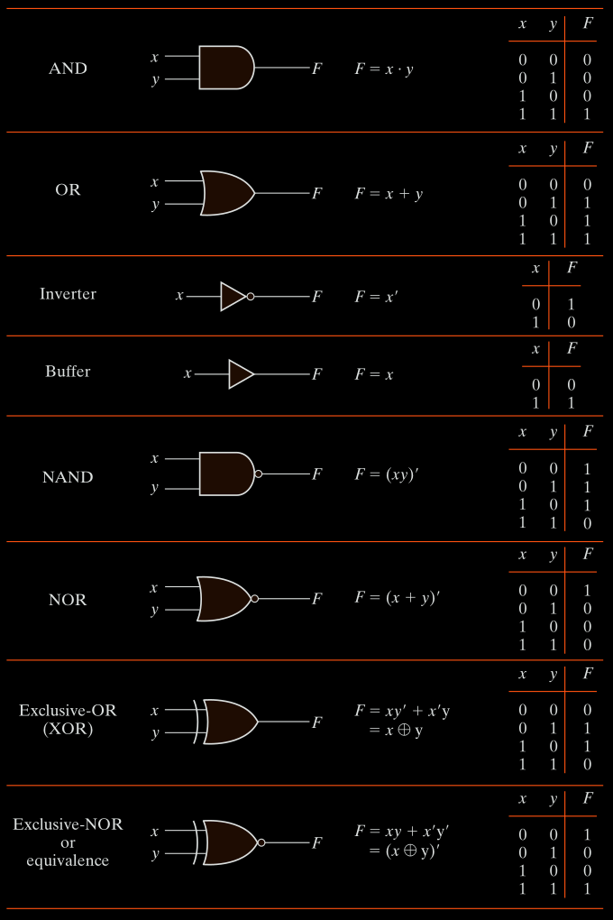
Figure 1.1 - Digital logic gates
Multi-Input Gates
Gates can have more than two inputs:
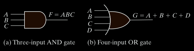
Figure 1.2 - Gates with multiple inputs.
AND
The AND logic function:
the output is 1 if input A and input B are both equal to 1 otherwise, the output is 0.
The algebraic operation symbol of the AND function is the same as the multiplication symbol of ordinary arithmetic. We can either use a dot between the variables like ($x \cdot y$) or concatenate the variables without an operation symbol between them like ($xy$)
AND gates may have more than two inputs, and by definition, the output is 1 if and
only if all inputs are 1.
OR
The OR logic function:
the output is 1 if input A or input B or both inputs are 1 otherwise, the output is 0. The algebraic symbol of the OR function is $+$ like ($x+y$) similar to arithmetic addition.
OR gates may have more than two inputs, and by definition, the output is 1 if any
input is 1.
Inverter & Buffer
The inverter circuit inverts the logic sense of a binary signal. It produces the NOT, or complement.
The algebraic symbol used for the logic complement is either ($x’$) or ($¬x$) or a bar over the variable symbol.
The small circle in the output of the graphic symbol of an inverter designates a logic complement. A triangle symbol by itself designates a buffer circuit.
A buffer does not produce any particular logic function since the binary value of the output is the same as the binary value of the input.
This circuit is used merely for power amplification. For example, a buffer that uses 3 volts for binary 1 will produce an output of 3 volts when its input is 3 volts. However, the amount of electrical power needed at the input of the buffer is much less than the power produced at the output of the buffer. The main purpose of the buffer is to drive other gates that require a large amount of power.
NAND
The NAND function is the complement of the AND function, as indicated by the graphic symbol, which consists of an AND graphic symbol followed by a small circle.
The designation NAND is derived from the abbreviation of NOT-AND.
NOR
The NOR gate is the complement of the OR gate and uses an OR graphic symbol followed by a small circle.
Both NAND and NOR gates may have more than two inputs.
XOR
The exclusive-OR gate has a graphic symbol similar to the OR gate except for the additional curved line on the input side.
The output of this gate is 1 if any input is 1 but excludes the combination when both inputs are 1.
The exclusive-OR function has its own algebraic symbol like ($x⊕y$) or can be expressed in terms of AND, OR, and complement operations as shown in Fig. 1-1
A more fitting name for the exclusive-OR operation would be an odd function, that is, its output is 1 if an odd number of inputs are 1. Thus in a three-input exclusive-OR (odd) function, the output is 1 if only one input is 1 or if all three inputs are 1.
XNOR
The exclusive-NOR is the complement of the exclusive-OR, as indicated by the small circle in the graphic symbol. The output of this gate is 1 only if both inputs are equal to 1 or both inputs are equal to 0.
The exclusive-OR and exclusive-NOR gates are commonly available with two inputs, and only seldom are they found with three or more inputs.
Boolean Algebra
Boolean algebra is an algebra that deals with binary variables and logic operations. The three basic logic operations are AND, OR, and complement.
Operator precedence when solving Boolean expressions: Parentheses > NOT > AND > OR
To qualify as a Boolean algebra, the elements and operations must satisfy six Huntington Postulates:
Huntington’s Six Postulates (Axioms)
Let x, y, and z be elements of set B (they are either 0 or 1 in the two-valued case). Then:
1. Closure
For all x, y in B, x + y is also in B.
For all x, y in B, x · y is also in B.
B is closed under +: If you apply + (OR) to any two elements in B, the result is still in B. Same thing but for · (AND).
2. Identity Elements
There exists an element 0 in B such that for all x:
x + 0 = 0 + x = x → (0 is identity for OR)
x + 0 = x so OR-ing with 0 doesn’t change the value.
There exists an element 1 in B such that for all x:
x · 1 = 1 · x = x → (1 is identity for AND)
x · 1 = x so AND-ing with 1 doesn’t change the value.
3. Commutative Laws
OR is commutative: x + y = y + x
AND is commutative: x · y = y · x
The order of operands doesn’t affect the result.
4. Distributive Laws
AND distributes over OR: x · (y + z) = (x · y) + (x · z)
OR distributes over AND: x + (y · z) = (x + y) · (x + z)
5. Complements
For every element x in B, there exists a complement x' in B such that:
x + x' = 1x · x' = 0
Complement is like the NOT operator. It flips the value (0' = 1, 1' = 0).
6. Existence of at Least Two Distinct Elements
There exist at least two elements x and y in B such that x ≠ y.
This ensures the algebra isn’t trivial, it must have at least two different elements. In two-valued Boolean algebra, these are 0 and 1.
Operator Truth Tables (For 2-Valued Boolean Algebra)
OR
| x | y | x + y |
|---|---|---|
| 0 | 0 | 0 |
| 0 | 1 | 1 |
| 1 | 0 | 1 |
| 1 | 1 | 1 |
AND
| x | y | x · y |
|---|---|---|
| 0 | 0 | 0 |
| 0 | 1 | 0 |
| 1 | 0 | 0 |
| 1 | 1 | 1 |
NOT (Complement)
| x | x' |
|---|---|
| 0 | 1 |
| 1 | 0 |
Proving the Postulates for {0, 1}
Let’s verify that the six postulates hold true for B = {0, 1}:
1. Closure:
All results of + and · from the tables are either 0 or 1, which are in B.
2. Identity:
x + 0 = x and x · 1 = x verified from tables.
3. Commutativity:
- OR:
0+1 = 1 = 1+0 - AND:
0·1 = 0 = 1·0
4. Distributivity:
Use a truth table to verify:
x · (y + z) = (x · y) + (x · z)x + (y · z) = (x + y) · (x + z)
Truth tables prove these hold for all combinations of x, y, z.
5. Complement:
0 + 1 = 1,0 · 1 = 0→1is complement of01 + 0 = 1,1 · 0 = 0→0is complement of1
6. Two Elements Exist:
Set B = {0, 1} obviously has two distinct elements.
Therefore, {0, 1}, with +, ·, and complement, forms a valid Boolean algebra.
Duality Principle
Every Boolean expression has a dual. You get it by:
- Swapping AND ( • ) ↔ OR ( + )
- Swapping
0↔1
Because Boolean algebra is symmetric in a way that mirrors logic in both directions.
BASIC THEOREMS (Derived from Postulates)
These are proven rules based on the postulates.
| Theorem | Statement | Dual |
|---|---|---|
| T1 | x + x = x |
x • x = x |
| T2 | x + 1 = 1 |
x • 0 = 0 |
| T3 (Involution) | (x')' = x |
Same |
| T4 (Associative) | x + (y + z) = (x + y) + z |
x • (y • z) = (x • y) • z |
| T5 (DeMorgan’s) | (x + y)' = x' • y' |
(x • y)' = x' + y' |
| T6 (Absorption) | x + x • y = x |
x • (x + y) = x |
Theorem 1
a:
$x + x = x$
b:
$x \cdot x = x$
Theorem 2
a:
$ x + 1 = 1 $
b:
$ x \cdot 0 = 0 $
Theorem 3 (Involution Law)
$(x’)’ = x$
Double negation returns to the original. Like saying:
Theorem 4 (Commutative and Associative Laws)
Commutative:
$ x + y = y + x $
$x \cdot y = y \cdot x $
Order doesn’t matter for AND or OR.
Associative:
$x + (y + z) = (x + y) + z $
$x \cdot (y \cdot z) = (x \cdot y) \cdot z $
Grouping doesn’t matter for AND or OR.
Theorem 5 (DeMorgan’s Laws)
It states that a NOR gate that performs the $(x + y)’$ function is equivalent to the function $(x’y’)$
Similarly, NAND function can be expressed by either $(xy)’$ or $(x’+y’)$
$(x + y)’ = x’ \cdot y’ $
$(x \cdot y)’ = x’ + y’ $
Instead of representing a NOR gate with an OR graphic symbol followed by a circle, we can represent it by an AND graphic symbol preceded by circles in all inputs.
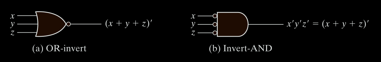
Figure 1.3 - Two graphic symbols for the NOR gate
Similarly, the NAND gate has also two distinct symbols, we can represent it by an OR graphic symbol preceded by circles in all inputs.
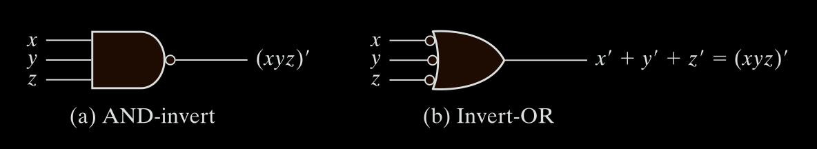
Figure 1.4 - Two graphic symbols for a three-input NAND gate
Theorem 6 (Absorption Laws)
$x + x \cdot y = x$
$x \cdot(x + y) = x$
Once you already have $x$, adding $xy$ (or multiplying $x$ by $(x+y)$) doesn’t change anything.
If $x$ is true, $xy$ doesn’t add any new information.
Other Logic Operations
Total Functions for 2 Binary Variables
-
If you have 2 binary variables (
x,y), there are 4 possible input combinations:- $00$
- $01$
- $10$
- $11$
-
Each function’s output is 4 bits long (one for each input row).
-
Since each bit can be either 0 or 1, the total number of functions is:
$2^4 = 16$ functions
These are listed below, with each function labeled $F_0$ to $F_{15}$.
Truth Table of All 16 Binary Functions
Each function is a column. The rows show what the output (F) would be for each input (x, y).
| x | y | F0 | F1 | F2 | F3 | F4 | F5 | F6 | F7 | F8 | F9 | F10 | F11 | F12 | F13 | F14 | F15 |
|---|---|---|---|---|---|---|---|---|---|---|---|---|---|---|---|---|---|
| 0 | 0 | 0 | 0 | 0 | 0 | 0 | 0 | 0 | 0 | 1 | 1 | 1 | 1 | 1 | 1 | 1 | 1 |
| 0 | 1 | 0 | 0 | 0 | 0 | 1 | 1 | 1 | 1 | 1 | 0 | 1 | 1 | 1 | 1 | 1 | 1 |
| 1 | 0 | 0 | 0 | 1 | 1 | 0 | 0 | 1 | 1 | 1 | 0 | 0 | 0 | 1 | 1 | 1 | 1 |
| 1 | 1 | 0 | 1 | 0 | 1 | 0 | 1 | 0 | 1 | 0 | 1 | 0 | 1 | 0 | 1 | 0 | 1 |
Meaning of Each Function
| Fn | Boolean Expression | Operator Symbol | Name | Comment |
|---|---|---|---|---|
| F0 | 0 | Null | Always 0 | |
| F1 | x · y | $x \cdot y$ | AND | Only 1 when x = y = 1 |
| F2 | x · y' | Inhibition | x AND NOT y | |
| F3 | x | Transfer | Just x | |
| F4 | x’ · y | Inhibition | y AND NOT x | |
| F5 | y | Transfer | Just y | |
| F6 | x · y’ + x’ · y | $x ⊕ y$ | XOR | 1 if x ≠ y |
| F7 | x + y | $x + y$ | OR | 1 if x = 1 or y = 1 |
| F8 | (x + y)' | $x ↓ y$ | NOR | NOT(x OR y) |
| F9 | x · y + x’ · y' | $(x ⊕ y)'$ | XNOR | 1 if x = y |
| F10 | y' | y' | NOT y | Complement of y |
| F11 | x + y' | x → y | Implication | If y, then x |
| F12 | x' | x' | NOT x | Complement of x |
| F13 | x’ + y | y → x | Implication | If x, then y |
| F14 | (x · y)' | $x ↑ y$ | NAND | NOT(x AND y) |
| F15 | 1 | Identity | Always 1 |
Integrated Circuits (IC)
Is built on a silicon chip (called a die) using a silicon semiconductor crystal. The chip contains electronic components (like transistors) used to build digital logic gates.
These gates are interconnected inside the chip to form desired digital circuits. The chip is placed in a plastic or ceramic package, and external pins are connected to the gates inside the chip.
Small packages: ~14 pins
Large packages: several thousand pins
Each IC has a numeric ID printed on it for identification.
Manufacturers provide Data books Catalogs Websites with technical details about their ICs.
Levels of Integration
Digital Integrated Circuits (ICs) are classified based on the number of logic gates they contain within a single package. This classification is known as Levels of Integration and has evolved over time with advancements in semiconductor technology.
| Level | Gates per Chip | Examples | Era |
|---|---|---|---|
| SSI | 1–10 | Basic logic gates | 1960s |
| MSI | 10–100 | Counters, MUX/DEMUX | Late 1960s–1970s |
| LSI | 100–10,000 | 8-bit CPUs, RAM | 1970s–1980s |
| VLSI | 10,000–1M | 32/64-bit CPUs, GPUs | 1980s–2000s |
| ULSI | 1M–billions | Multi-core CPUs, AI chips | 2000s–present |
| WSI | Wafer-level | Cerebras WSE | Future/Experimental |
Computer-Aided Design (CAD)
ICs are created by projecting light patterns onto silicon wafers. Wafers are coated with a photoresist. Light exposure hardens or softens the photoresist.
Etching removes parts, leaving patterns for: Transistors, Gates, Doping implants atoms to change electrical properties.