Combinational Circuit
A digital logic circuit where the output is solely determined by the current input combination (no memory or feedback).
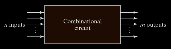
Figure 1.1 - Block diagram of combinational circuit.
Half-Adder
A combinational circuit that performs the arithmetic addition of two bits is called
a half-adder.
One that performs the addition of three bits (two significant bits
and a previous carry) is called a full-adder.
The name of the former stems from the fact that two half-adders are needed to implement a full-adder.
The input variables of a half-adder are called the augend and addend bits.
The output variables the sum and carry.
It is necessary to specify two output variables because the sum of 1 + 1 is binary 10, which has two digits. We assign symbols x and y to the two input variables, and S (for sum) and C (for carry)
The truth table for the half-adder is:
| x | y | Sum (S) | Carry (C) |
|---|---|---|---|
| 0 | 0 | 0 | 0 |
| 0 | 1 | 1 | 0 |
| 1 | 0 | 1 | 0 |
| 1 | 1 | 0 | 1 |
The C output is 0 unless both inputs are 1. The S output represents the least significant bit of the sum. The Boolean functions for the two outputs can be obtained directly from the truth table:
$S = x⊕y$
$C = x\cdot y$
The logic diagram is shown in Fig. 1-2 It consists of an exclusive-OR gate and an AND gate.
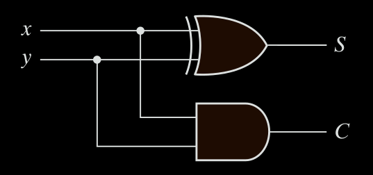
Figure 1.2 - Half-Adder circuit.
Full-Adder
A combinational circuit that forms the arithmetic sum of three input bits. It consists of three inputs and two outputs. Two of the input variables, denoted by x and y, represent the two significant bits to be added. The third input, z, represent the carry from the previous lower significant position.
Two outputs are necessary because the arithmetic sum of three binary digits ranges in value from 0 to 3, and binary 2 or 3 needs two digits. The two outputs are designated by the symbols S (for sum) and C (for carry).
The binary variable S gives the value of the least significant bit of the sum.
The binary variable C gives the output carry.
The truth table of the full-adder is:
| A | B | Cin | Sum (S) | Cout |
|---|---|---|---|---|
| 0 | 0 | 0 | 0 | 0 |
| 0 | 0 | 1 | 1 | 0 |
| 0 | 1 | 0 | 1 | 0 |
| 0 | 1 | 1 | 0 | 1 |
| 1 | 0 | 0 | 1 | 0 |
| 1 | 0 | 1 | 0 | 1 |
| 1 | 1 | 0 | 0 | 1 |
| 1 | 1 | 1 | 1 | 1 |
The value of the output variables are determined from the arithmetic sum of the input bits. When all
input bits are 0, the output is 0. The S output is equal to 1 when only one input
is equal to 1 or when all three inputs are equal to 1 . The C output has a carry
of 1 if two or three inputs are equal to 1.
One possible expression for C is
$C = x\cdot y + (x’y +ry’)z$
Realizing that x’y +xy = x⊕y and including the expression for output S , we obtain the two Boolean expressions for the full-adder:
$S = x ⊕ y ⊕ z$
$C = x\cdot y + (x⊕y)z$
The logic diagram of the full-adder is drawn in Fig. 1-3 Note that the full adder circuit consists of two half-adders and an OR gate.
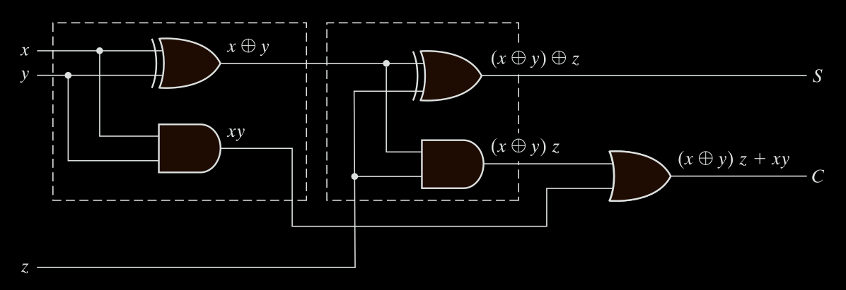
Figure 1.3 - Full-Adder circuit.
Sequential Circuits
A sequential circuit combines: combinational circuit and Memory elements (flip-flops or latches) to store binary information.
Stores a state: The current data in the memory elements. Unlike combinational circuits, the output depends on the history of inputs (because of the stored state).
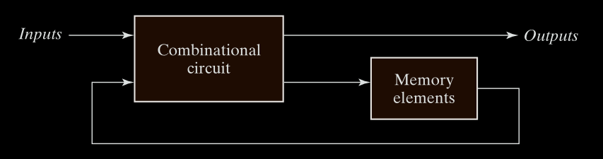
Figure 1.4 - Block diagram of Sequential Circuit.
Synchronous Sequential Circuits
- State changes occur only at discrete time intervals.
- Controlled by a clock signal (clk), a periodic square wave.
- Common and widely used in practice (CPUs, digital systems).
- Easy to analyze and design because of predictable timing.
Asynchronous Sequential Circuits
- State changes can occur at any time, triggered by input changes.
- Use time-delay or feedback-based storage instead of clocking.
- Often unstable, harder to design and debug.
- Not covered in this book due to complexity.
Synchronous Sequential Circuit Operation
Clock
- A clock generator produces periodic pulses.
- Flip-flops only respond during clock transitions.
Feedback Loop
- Flip-flop outputs feed back into combinational logic.
- Next state is computed before the clock pulse and loaded on its edge.
- Important to ensure propagation delays are managed to avoid incorrect data being latched.
State Transition
- The circuit moves from one state to another only when the clock ticks.
- Between clock pulses, outputs may change, but flip-flops don’t update.
Latches vs Flip-Flops
Latches
- Level-sensitive: State can change as long as enable signal is active.
- Can change state multiple times during a level.
Flip-Flops
- Edge-sensitive: Change state only on clock edge.
- More reliable in synchronous designs.
| Feature | Latch | Flip-Flop |
|---|---|---|
| Triggering | Level-triggered | Edge-triggered |
| Clock input? | Not always, but often has Enable (EN) | Always triggered by a Clock edge |
| Sensitive to | While Enable = 1 | Only on clock edge (↑ or ↓) |
| Timing | Can change multiple times while EN = 1 | Changes once per clock edge |
SR (Set-Reset) Latch
a basic memory element in digital electronics that can store 1 bit of data (0 or 1). It has two stable states and is built using cross-coupled NOR gates or NAND gates.
NOR-based SR Latch:
Constructed using 2 cross-coupled NOR gates.
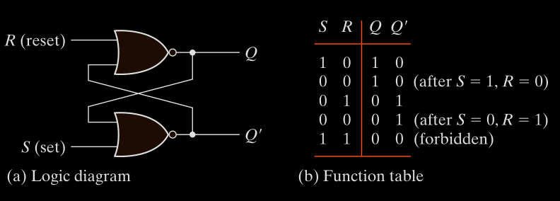
Figure 1.5 - SR latch with NOR gates.
Output States:
| S | R | Q (next) | Description |
|---|---|---|---|
| 0 | 0 | No change | Hold state |
| 1 | 0 | Q = 1 | Set |
| 0 | 1 | Q = 0 | Reset |
| 1 | 1 | Invalid | Forbidden |
NAND-based SR Latch:
Similar logic, but uses active-low inputs (denoted S’ and R’).
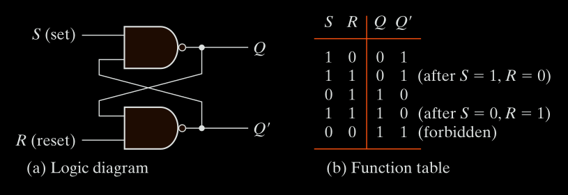
Figure 1.6 - SR latch with NAND gates.
Input Logic:
| S' | R' | Q (next) | Description |
|---|---|---|---|
| 1 | 1 | No change | Hold |
| 0 | 1 | Q = 1 | Set |
| 1 | 0 | Q = 0 | Reset |
| 0 | 0 | Invalid | Forbidden |
SR Latch with Enable
Adds an enable input (En) to allow control of when S and R affect the circuit.
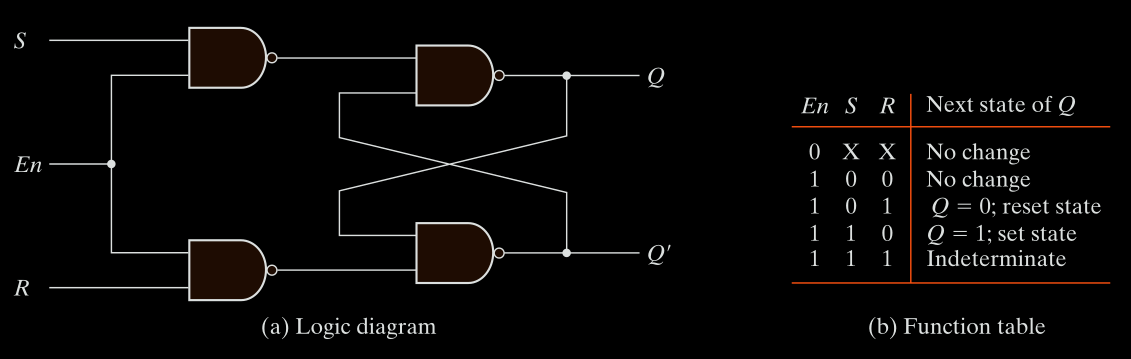
Figure 1.7 - SR latch with control input.
D Latch (Transparent Latch)
Solves the SR latch indeterminate condition.
Has only 2 inputs: D (Data) and En (Enable).
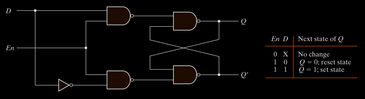
Figure 1.8 - D latch.
Construction:
- D connected to S.
- NOT D connected to R.
Behavior:
| En | D | Q (next) | Description |
|---|---|---|---|
| 0 | X | No change | Hold state |
| 1 | 0 | Q = 0 | Reset |
| 1 | 1 | Q = 1 | Set |
While En = 1 output Q follows D → latch is “transparent”.
When En = 0 latches the last D value.
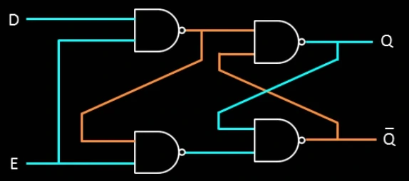
Figure 1.9 - D latch in a differnt way.
Graphic Symbols for Latches
Latches use rectangular blocks.
May include:
- Control input (En).
- Inputs (S/R or D).
- Outputs (Q and possibly Q’).
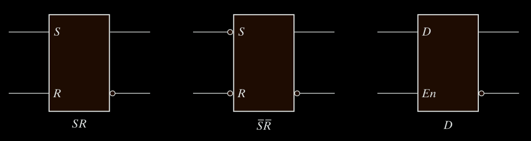
Figure 2.1 - Graphic symbols for latches.
Flip-Flops
The storage elements employed in clocked sequential circuits are called flip-flops. A flip-flop is a binary cell capable of storing one bit of information. It has two outputs, one for the normal value and one for the complement value of the bit stored in it.
A flip-flop maintains a binary state until directed by a clock pulse to switch states. and it’s an edge-triggered storage element.
It only updates its output on the edge (transition) of the clock, either rising edge (0 → 1) or falling edge (1 → 0).
It stores one bit of data (0 or 1).
It is triggered (changes state) by a control input, usually called a clock.
The D latch with a pulsed control input becomes a flip-flop, as it now only updates output when the control (enable or clock) is at logic 1.
Edge Triggered Flip-Flops
The most common type of flip-flop used to synchronize the state change during a clock pulse transition is the edge-triggered flip-flop. In this type of flip-flop, output transitions occur at a specific level of the clock pulse. When the pulse input level exceeds this threshold level, the inputs are locked out so that the flip-flop is unresponsive to further changes in inputs until the clock pulse returns to 0 and another pulse occurs.
Some edge-triggered flip-flops cause a transition on the rising edge of the clock signal (positive-edge transition), and others cause a transition on the falling edge (negative-edge transition).
Fig. 2-3 shows the clock pulse signal in a positive-edge-triggered D flip-flop.
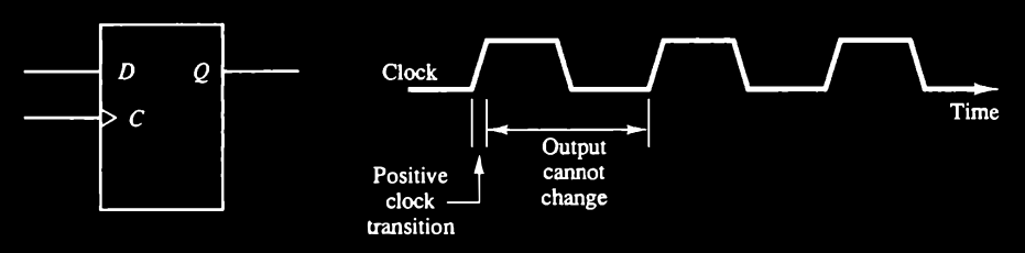
Figure 2.3 - Positive-edge-triggered D flip-flop.
The value in the D input is transferred to the Q output when the clock makes a positive transition. The output cannot change when the clock is in the 1 level, in the 0 level, or in a transition from the 1 level to the 0 level.
The effective positive clock transition includes a minimum time called the setup time in which the D input must remain at a constant value before the transition, and a definite time called the hold time in which the D input must not change after the positive transition. The effective positive transition is usually a very small fraction of the total period of the clock pulse.
Fig. 2-4 shows the corresponding graphic symbol and timing dia gram for a negative-edge-triggered D flip-flop.
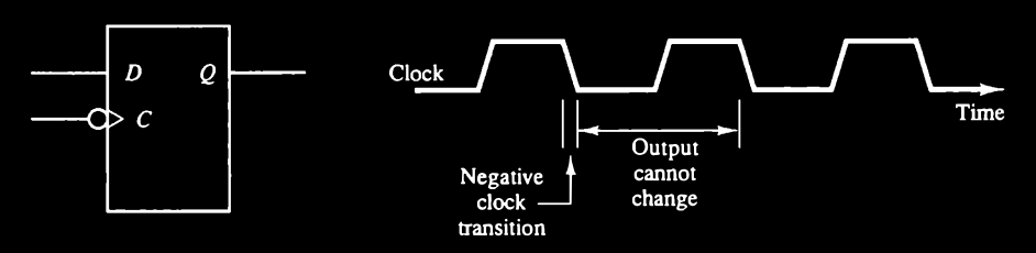
Figure 2.4 - Negative-edge-triggered D flip-flop.
The graphic symbol includes a negation small circle in front of the dynamic indicator at the C input. This denotes a negative-edge-triggered behavior. In this case the flip-flop responds to a transition from the 1 level to the 0 level of the clock signal.
SR Flip-Flop
The graphic symbol of the SR flip-flop is shown in Fig. 2-5

Figure 2.5 - SR flip-flop Graphic symbol.
It has three inputs, labeled S (for set), R (for reset), and C (for clock). It has an output Q and sometimes the flip-flop has a complemented output, which is indicated with a small circle at the other output terminal. There is an arrowhead-shaped symbol in front of the letter C to designate a dynamic input. The dynamic indicator symbol denotes the fact that the flip-flop responds to a positive transition (from 0 to 1) of the input clock signal.
The operation of the SR flip-flop:
If there is no signal at the clock input C, the output of the circuit cannot change irrespective of the values at inputs S and R.
If both S and R are 0 during the clock transition, the output does not change.
Only when the clock signal changes (from 0 to 1) can the output be affected according to the values in inputs S and R. If S = 1 and R = 0 when C changes from 0 to 1, output Q is set to 1.
If S = 0 and R = 1 when C changes from 0 to 1, output Q is cleared to 0.
When both S and R are equal to 1, the output is unpredictable and may go to either 0 or 1, depending on internal timing delays that occur within the circuit.
Here’s The operation of the SR flip-flop in tabular form:
| S | R | Q ( t + 1 ) | |
|---|---|---|---|
| 0 | 0 | Q(t) | No change |
| 0 | 1 | 0 | Clear to O |
| 1 | 0 | 1 | Set to 1 |
| 1 | 1 | ? | Indeterminate |
The S and R columns give the binary values of the two inputs.
Q(t) is the binary state of the Q output at a given time (referred to as present state).
Q(t + 1) is the binary state of the Q output after the occurrence of a clock transition (referred to as next state).
If S = R = 0, a clock transition produces no change of state [Q(t + 1) = Q(t)]. If S = 0 and R = 1 , the flip-flop goes to the 0 (clear) state. If S = 1 and R = 0, the flip-flop goes to the 1 (set) state.
The SR flip-flop should not be pulsed when S = R = 1 since it produces an indeterminate next state.
This indeterminate condition makes the SR flip-flop difficult to manage and therefore it is seldom used in practice.
D Flip-Flop
The graphic symbol of the D flip-flop are shown in Fig. 2-6
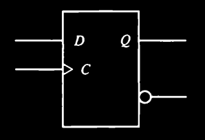
Figure 2.6 - D flip-flop Graphic symbol.
The D (data) flip-flop is a slight modification of the SR flip-flop. An SR flip-flop is converted to a D flip-flop by inserting an inverter between S and R and assigning the symbol D to the single input.
The D input is sampled during the occurrence of a clock transition from 0 to 1.
If D = 1, the output of the flip-flop goes to the 1 state, but if D = 0, the output of the flip-flop goes to the 0 state.
| D | Q ( t + 1 ) | |
|---|---|---|
| 0 | 0 | Clear to 0 |
| 1 | 1 | Set to 1 |
From the characteristic table we note that the next state Q(t + 1) is determined from the D input.
The relationship can be expressed by a characteristic equation:
$Q(t + 1) = D$
This means that the Q output of the flip-flop receives its value from the D input every time that the clock signal goes through a transition from 0 to 1.
Note that no input condition exists that will leave the state of the D flip-flop unchanged.
Although a D flip-flop has the advantage of having only one input (excluding C), it has the disadvantage that its characteristic table does not have a “no change” condition Q(t + 1) = Q(t).
The “no change” condition can be accomplished either by disabling the clock signal or by feeding the
output back into the input, so that clock pulses keep the state of the flip-flop unchanged.
Master–Slave D Type Flip-Flop
Another type of flip-flop used in some systems is the master-slave flip
flop. This type of circuit consists of two flip-flops. The first is the master, which
responds to the positive level of the clock, and the second is the slave, which
responds to the negative level of the clock.
The result is that the output changes during the 1-to-0 transition of the clock signal. The trend is away from the use of master-slave flip-flops and toward edge-triggered flip-flops.
Flip-flops available in integrated circuit packages will sometimes provide special input terminals for setting or clearing the flip-flop asynchronously. These inputs are usually called “preset” and “clear.” They affect the flip-flop on a negative level of the input signal without the need of a clock pulse. These inputs are useful for bringing the flip-flops to an initial state prior to its clocked operation.
This is a common way to build an edge-triggered D flip-flop using two D latches and an inverter.
As shown in Fig. 2-7
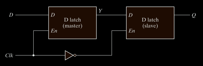
Figure 2.7 - Master–slave D flip-flop.
Architectures
Computer architecture refers to the design and structure of a computer system, how its components (CPU, memory, input/output) work together, it defines how data moves, how instructions are executed, and how memory is organized.
There are different types of architectures:
Von Neumann Architecture
Single Memory for Code + Data, Programs and data share the same memory space.
Code Injection Possible, since data and code are in the same memory.
Attackers reuse existing code (“gadgets”) because everything is in one memory space, Return-Oriented Programming (ROP)
Harvard Architecture (Rare in General-Purpose CPUs)
Separate Memory for Code + Data.
Can’t directly inject code into data regions, no shellcode execution from stack/heap.
Modified Harvard Architecture (Modern Hybrid)
Split Memory but Allows Tricks, Data Execution Prevention (DEP), Side-Channel Attacks Still Work