Memory
A memory unit is a device used in digital systems to store binary data and later retrieve it when needed for processing. It works in two main directions:
- Storing data when it comes from an input or from processing.
- Retrieving data to use in processing or to send to an output device.
Memory consists of many cells that can store binary values (0s and 1s).
Each cell stores 1 bit, and groups of cells form words or bytes (more on this below).
There are two main types of memory:
RAM (Random-Access Memory)
Can read and write data.
Used to store temporary data during processing.
A RAM unit is made of:
- Storage cells to hold data.
- Circuits to handle reading and writing.
Any memory location can be accessed directly and in equal time, regardless of position.
This is unlike magnetic tape, which reads data sequentially (you wait to reach the position).
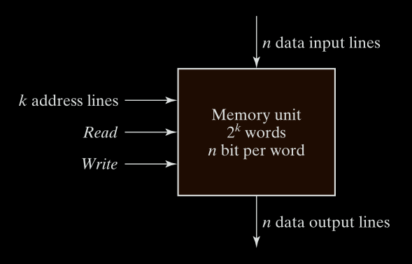
Figure 1.2 - ROM block diagram.
- n data input lines: To write data into memory.
- n data output lines: To read data out.
- k address lines: To select which word (out of all available) to read or write.
ROM (Read-Only Memory)
Is a type of nonvolatile memory where binary data is permanently stored during manufacturing or programming. Can only be read, not written to (after manufacturing/programming).
It is a combinational logic device with:
- Inputs: Address lines (k bits)
- Outputs: Data lines (n bits)
- No data inputs: cannot be written during normal operation.
Once data is programmed, it persists even without power.
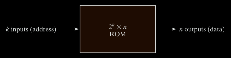
Figure 1.2 - Four‐bit register with parallel load
A ROM with k input lines and n output lines stores 2ᵏ words of n bits each.
Address lines (inputs) select one of the 2ᵏ words.
Data outputs present the word stored at the selected address.
Programmable Logic Devices (PLDs)
A PLD is a chip that can be custom-programmed to implement a specific logic function.
ROM is a type of PLD (Programmable Logic Device).
ROM Programming
Programming ROM means burning the correct data (bits) into the hardware. Internally, ROM uses elements like fuses. Initially, all paths (fuses) are intact. Programming involves blowing fuses (disabling certain paths) to create a desired fixed pattern.
Other PLD Types
- PLA (Programmable Logic Array)
- PAL (Programmable Array Logic)
- FPGA (Field-Programmable Gate Array)
Each of these lets you design logic circuits without physical rewiring.
PLD Internals
A PLD can contain hundreds to millions of logic gates.
Gates are connected through programmable paths (like fuses).
Gate Symbol for Array Logic
To represent PLDs compactly, a special symbology is used:

Figure 1.3 - Conventional and array logic diagrams for OR gate.
Instead of drawing every individual input into a gate, we show:
- One main line going into the gate (e.g., OR gate).
- Many small lines crossing perpendicularly, representing inputs connected via fuses.
This is used for both AND and OR gates in PLD diagrams.
Words and Bytes
Word
A group of bits treated as a unit. It’s the basic item stored or retrieved.
Words can represent:
- Numbers
- Instructions
- Characters
- Any other binary-coded information
Byte
A group of 8 bits.
- A 16-bit word = 2 bytes
- A 32-bit word = 4 bytes
Memory Capacity measured in bytes.
A memory with 1K words of 16 bits = 2K bytes (because 1 word = 2 bytes).
Memory Size and Addressing
A memory is described as: (Number of words) × (Number of bits per word)
- Number of words
The number of words = how many unique locations the memory has.
- Number of bits per word
This is how many bits (0s and 1s) are stored in each word.
Memory Is Made of Words
A word is the basic unit of memory that holds a fixed number of bits.
For example:
-
In a
1K × 16memory:- There are 1K = 1024 words.
- Each word is 16 bits long (can store 16 bits of binary data).
So in total:
The whole memory can store 1024 × 16 = 16,384 bits of data.
Addressing the Words
Every word has a unique address, so the computer knows where to find or store it.
If the memory has 2^k words, then we need k bits for the address.
Example:
- Word 0 → first word
- Word 1 → second word
- …
- Word 1023 → last word in a 1K memory
To select a word, you use binary addresses.
So:
- word 0 =
0000000000 - Word 1 =
0000000001 - Word 1023 =
1111111111
This is how the memory knows which word you’re referring to.
Example:
If there are (1k = 1024) words, how many addresses do we need?
- We need to count from 0 to 1023.
- That’s 1024 total addresses, and you can represent that in 10 bits, why?
because: $2^{10} = 1024$
So, a memory with 1K (1024) words needs 10 address bits.
Example: Memory Unit: 1K × 16
This means:
- 1K = 1024 words
- Each word = 16 bits
So this memory:
- Has 1024 addressable locations (words)
- Needs 10 address bits (because $2^{10} = 1024$)
- Each location stores 16 bits
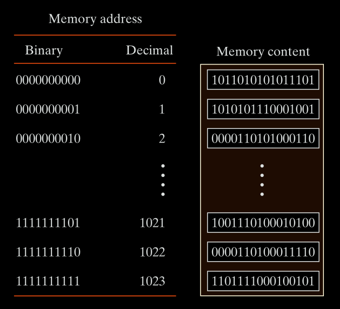
Figure 1.4 - Contents of a 1024 * 16 memory.
Address Lines
Address lines are the number of bits in the address.
-
If a memory has 1024 (1K = 2¹⁰) words, it needs 10 address lines (bits).
-
These 10 lines can represent any number from 0 to 1023 in binary.
-
Each word has its own unique address, so the number of addresses = number of words
So:
If a memory has $m$ words, you need $k$ address lines such that: $$ \boxed{2^k≥m} $$
This ensures you can uniquely address every word in memory.
Your computer (or any digital system) assigns a unique binary number to each memory word (location).
To do that, it needs:
$log_2$ (number of memory locations) bits to uniquely address them all
So if your computer has 4096 memory locations (words), then:
$log_2(4096)=12$ bits
This means:
-
Every memory address is 12 bits wide.
-
It takes 12 address lines (physical wires) on the address bus to select a location.
But why (≥) and not (=)
Yes, in most perfect cases, memory sizes are powers of 2.
If you have 1K = 1024 = 2¹⁰ words, you need exactly 10 address lines, because:
$2^{10} = 1024$
This is neat and efficient. Nothing is wasted.
But Sometimes 2^k > m
What if you have 1000 words not 1024 words
You still need enough address lines to cover all 1000 words.
So you find the smallest k such that:
$2^k ≥ 1000$
Let’s try values of k:
- 2⁹ = 512 ❌
- 2¹⁰ = 1024 ✅
Even though 1024 is more than 1000, we must use 10 address lines to make sure we can access all 1000 memory locations.
So:
$$ \boxed{2^{10} = 1024 \geq 1000} $$
Another Example: Memory Unit: 64K × 10
$64K$ $=$ $2^{16}$ words
$k = 16$ address bits
Each word $=$ $10$ bits
So this memory:
- Can store 64K = 65,536 words
- Each word has 10 bits
- Needs 16 address lines (address bits)
Total number of bits = 65,536 × 10 = 655,360 bits
Data Lines
Data lines carry the actual bits of a word.
-
If each word is 16 bits, then there are 16 data input lines and 16 data output lines.
-
So when you read or write, you’re sending or receiving 16 bits at once.
Writing and Reading in Memory
Write Operation (Storing Data)
To write a new word into memory:
- Apply the binary address of the desired word to the address lines.
This selects where in memory the data will be written.
- Apply the data bits that must be stored in memory to the data input lines.
These are the actual bits you want to store.
- Activate the write input.
This tells the memory to perform the write operation.
The memory unit will then take the bits from the input data lines and store them in the word specified by the address lines.
Read Operation (Retrieving Data)
To read a word already stored in memory:
- Apply the binary address of the desired word to the address lines.
This selects which word to read.
- Activate the read input.
This tells the memory to perform the read operation.
The memory unit will then take the bits from the word that has been selected by the address and apply them to the output data lines.
Control Signals
In practice, many commercial memory chips use a slightly different setup for control inputs.
Instead of separate Read and Write lines, they often use:
- Memory Enable (also called Chip Select)
- Read/Write (R/W) line
Control Inputs to Memory Chip
| Memory Enable | Read/Write | Operation |
|---|---|---|
| 0 | X (don’t care) | No operation (chip disabled) |
| 1 | 0 | Write to selected word |
| 1 | 1 | Read from selected word |
Explanation:
-
Memory Enable = 0 → Chip is not selected. No operation takes place, even if R/W is 0 or 1.
-
Memory Enable = 1, Read/Write = 0 → Perform a write operation.
-
Memory Enable = 1, Read/Write = 1 → Perform a read operation.
Why Use Memory Enable
In large systems, multiple memory chips may be used together. The Memory Enable (ME) or Chip Select (CS) line is crucial for:
- Selecting which individual chip should respond to an operation.
- Preventing conflicts when many chips are connected to the same bus.
Only the chip with ME = 1 will participate, others stay inactive.
Registers
A register is a group of flip-flops with each flip-flop capable of storing one bit of information.
An n bit register has a group of n flip-flops and is capable of storing any binary information of n bits. In addition to the flip-flops, a register may have combinational gates that perform certain data-processing tasks. In its broadest definition, a register consists of a group of flip-flops and gates that effect their transition.
The simplest register is one that consists only of flip-flops, with no external gates. Fig. 1-5 shows such a register constructed with four D flip-flops.
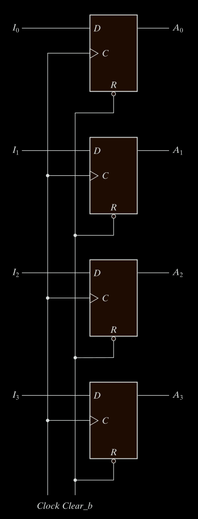
Figure 1.5 - 4-bit register.
The common clock input triggers all flip-flops on the rising edge of each pulse, and the binary data available at the four inputs are transferred into the 4-bit register. The four outputs can be sampled at any time to obtain the binary information stored in the register. The clear input goes to a special terminal in each flip-flop. When this input goes to 0, all flip-flops are reset asynchronously. The clear input is useful for clearing the register to all O’s prior to its clocked operation. The clear input must be maintained at logic 1 during normal clocked operation.
Note that the clock signal enables the D input but that the clear input is independent of the clock.
When you use latches in a system where outputs feed back into inputs (like in most sequential circuits), the outputs can keep changing as long as Enable is 1. That’s a feedback loop that never settles. This creates a feedback loop that can cause unstable behavior, as the output keeps changing while Enable = 1. That’s why we replace latches with flip-flops, which only update on a clock edge, so everything updates at the same time, cleanly and predictably.
You should not control flip-flops by gating the clock because:
- It introduces variable delays.
- Flip-flops may get clocked at different times.
- That causes timing mismatches = system instability or bugs.
it is advisable to control the operation of the register with the D inputs, rather than controlling the clock in the C inputs of the flip‐flops. This creates the effect of a gated clock, but without affecting the clock path of the circuit.
Counters
A type of register that cycles through a sequence of states (usually counting up or down).
Register Load
The transfer of new information into a register is referred to as loading the register. If all the bits of the register are loaded simultaneously with a common clock pulse transition, we say that the loading is done in parallel . A clock transition applied to the C inputs of the register of Fig. 1-1 will load all four inputs in parallel. In this configuration, the clock must be inhibited from the circuit if the content of the register must be left unchanged.
Registers are directly within the CPU, meaning no bus delay, no memory access time, and no memory bandwidth usage. They are the fastest type of memory in the system.
Instructions operating on registers typically execute in one cycle, while memory-based operations take multiple cycles.
Register with Parallel Load
Now let’s look at a smarter version: Fig. 1-6 the four-bit register with parallel load.
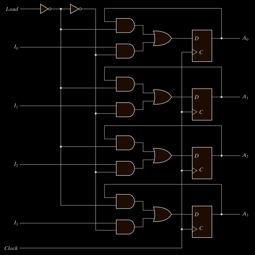
Figure 1.6 - Four‐bit register with parallel load.
Why Parallel Load
In synchronous systems, a master clock sends pulses to every component. We want to control when new data is loaded into a register. This is done using a load signal.
What’s Happening in This Register
It has the same 4 D flip-flops. It adds:
- A load control line.
- A MUX (multiplexer) per flip-flop to choose between.
In a register with a load control, the register contents only update when Load = 1 and clock edge occurs. This behavior requires that:
The MUX selects either:
- current output (
Qno change) - new data input (
Dload)
When Load = 1, the MUX passes new input data to the flip-flop. When Load = 0, the MUX feeds back the current output Q, maintaining the value.
This selective loading mechanism allows controlled updates on clock edges without gating the clock itself.
That’s why every bit needs a MUX before the D flip-flop.
This avoids relying on clock gating (which is risky).
Processor Registers
These are registers within the CPU, and they’re usually divided by function:
Processor registers can be specified by assigning to the instruction another binary code of k bits that specifies one of 2^k registers.
Registers are few, and each has a name (like R0, R1, …, R7)
If you have 8 registers, you need 3 bits to select one (because 2³ = 8).
So the instruction may have a 3-bit field for each register operand.
Instruction Code
An instruction code is a group of bits that tells the computer which operation to perform. It often includes which data to use, and where to store results.
Each instruction in memory consists of:
- Operation code (opcode): What to do?
- Operands: On what data to operate?
- (Optional) Destination: Where to store the result.
Operation Code (Opcode)
This is the core part of the instruction. It’s a few bits that specify the type of operation.
Example:
If your computer supports 64 operations, then how many bits do you need for the opcode?
You need log₂(64) = 6 bits because:
- 6 bits can represent
2⁶ = 64different values. - So, each opcode can uniquely identify one of those 64 operations.
Suppose:
110010= ADD operation.- When this is read by the control unit, it understands: “This instruction means add.”
Examples:
| Operation | Opcode (in binary) |
|---|---|
| ADD | 110010 |
| SUB | 100101 |
| LOAD | 000001 |
The control unit will decode this part and translate it into internal actions.
To perform operations like ADD you need data.
That data is:
- Either in registers
- Or in memory
So the instruction code must point to:
- The location of operands (data to operate on)
- And where to put the result
That’s because operations like ADD are meaningless unless you know:
- WHAT to add (A + B)
- WHERE to get A and B
- WHERE to store the result
So the instruction must contain this information, encoded in binary fields.
Then if you want the data from memory, you must tell the CPU where in memory the data is.
So the instruction code will contain a memory address field, telling the CPU to get data from that address.
From opcode to micro-operation
The instruction is high-level (like “ADD”). But inside the CPU, are needed to make that happen, these are called micro-operation.
so ADD is a micro-operation To actually do the addition, the CPU performs multiple micro-operation, like:
- Fetch operand A from register R1.
- Fetch operand B from register R2.
- Send both to the ALU.
- Store result in register R3.
These micro-operation are controlled by a special part of the CPU called the control unit.
Once the instruction is fetched:
- The control unit decodes the opcode.
- It then activates signals in a specific sequence to perform the needed micro-operation.
- These signals guide data movement between registers, memory, ALU, etc.
Stored Program Organization
The simplest way to organize a computer is to have one processor register and an instruction code format with two parts.
The first part specifies the operation to be performed.
The second specifies an address. The memory address tells the control where to find an operand in memory. This operand is read from memory and used as the data to be operated on together with the data stored in the processor register.
Fig. 1-7 depicts this type of organization. In the memory Instructions are stored in one section of memory and data in another.
For a memory unit with $4096 × 16$ words we need $12$ bits to specify an address since $2^{12} = 4096$ If we store each instruction code in one 16-bit memory word, we have available 4 bits for the operation code (abbreviated opcode) to specify one out of 16 possible operations, and 12 bits to specify the address of an operand.
The control reads a 16-bit instruction from the program portion of memory. It uses the 12-bit address part of the instruction to read a 16-bit operand from the data portion of memory. It then executes the operation specified by the operation code.
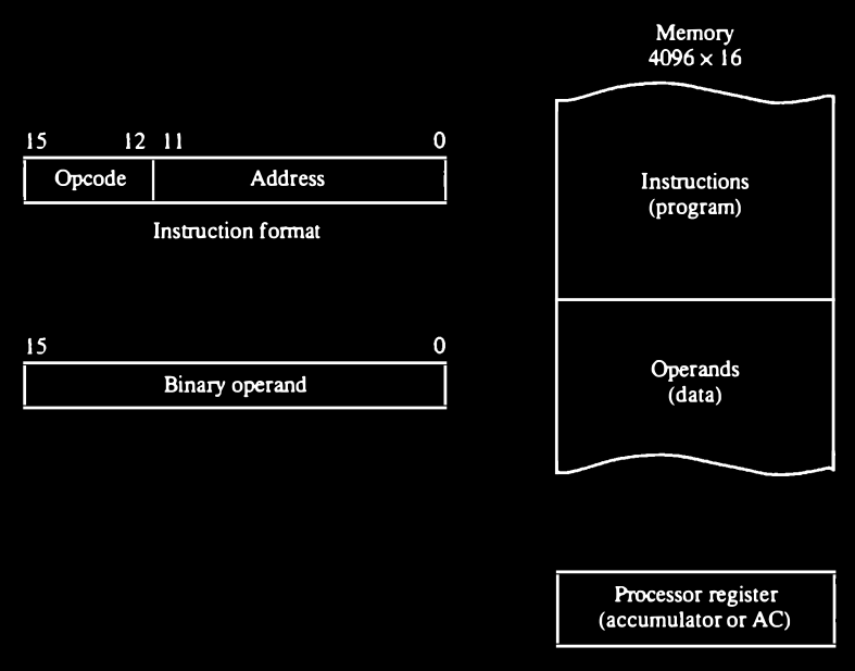
Figure 1.7 - Stored program organization.
Computers that have a single-processor register usually assign to it the name accumulator and label it AC.
The operation is performed with the memory operand and the content of AC. If an operation in an instruction code does not need an operand from memory, the rest of the bits in the instruction can be used for other purposes.
For example, operations such as clear AC, complement AC, and increment AC operate on data stored in the AC register. They do not need an operand from memory. For these types of operations, the second part of the instruction code (bits 0 through 11) is not needed for specifying a memory address and can be used to specify other operations for the computer.
Indirect Address
It is sometimes convenient to use the address bits of an instruction code not
as an address but as the actual operand. When the second part of an instruction
code specifies an operand, the instruction is said to have an immediate
operand. When the second part specifies the address of an operand, the
instruction is said to have a direct address. This is in contrast to a third
possibility called indirect address where the bits in the second part of the
instruction designate an address of a memory word in which the address of
the operand is found.
One bit of the instruction code can be used to distinguish between a direct and an indirect address. As an illustration of this configuration, consider the instruction code format shown in Fig. 1-8(a) It consists of a 3-bit operation code, a 12-bit address, and an indirect address mode bit designated by I.
The mode bit is 0 for a direct address and 1 for an indirect address.
A direct address instruction is shown in Fig. 1-8(b) It is placed in address 22 in memory. The I bit is 0, so the instruction is recognized as a direct address instruction. The opcode speci
fies an ADD instruction, and the address part is the binary equivalent of 457.
The control finds the operand in memory at address 457 and adds it to the
content of AC. The instruction in address 35 shown in Fig. 1-8(c) has a mode
bit I = 1. Therefore, it is recognized as an indirect address instruction. The
address part is the binary equivalent of 300. The control goes to address 300
to find the address of the operand. The address of the operand in this case is
1350. The operand found in address 1350 is then added to the content of AC.
The indirect address instruction needs two references to memory to fetch an
operand. The first reference is needed to read the address of the operand; the
second is for the operand itself. We define the effective address to be the address
of the operand in a computation-type instruction or the target address in a
branch-type instruction. Thus the effective address in the instruction of Fig. 1-8(b) is 457 and in the instruction of Fig. 1-8(c) is 1350.
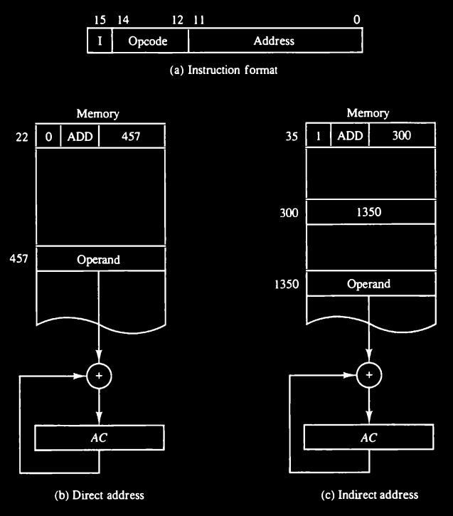
Figure 1.8 - Demonstration of direct and indirect address.
The memory word that holds the address of the operand in an indirect address instruction is used as a pointer to an array of data. The pointer could be placed in a processor register instead of memory.
Recap the Core Concepts
You’re dealing with 3 types of addressing:
- Immediate addressing: operand is inside the instruction (rare in this system).
- Direct addressing: instruction contains address of operand.
- Indirect addressing: instruction contains address of a memory word that contains the real operand address
Say you have this instruction in memory at address 35:
I = 1 (indirect mode)
Opcode = ADD
Address = 300
What Happens in Execution:
Because I = 1 this is indirect addressing. So the value 300 is not the operand. Instead:
- The control unit goes to memory address 300.
- It reads the content of memory[300], let’s say this is 1350.
- Now, it goes to memory[1350] and retrieves the actual operand.
- Finally, it adds that operand to AC.
The word at address 300 contains the value 1350
The word at address 1350 is the actual operand → for example the number 42 stored there.
Effective Address vs Operand
- Effective address = 1350 (final memory location used for actual data)
- Operand = value at memory[1350], for example 42
- Memory[300] = pointer to the operand
Memory word that holds the address of the operand this is memory[300] = 1350 So 300 is holding a pointer to where the actual operand lives.
This pointer (1350) could point to:
- A single operand
- Or the start of an array (if used that way).
If pointer to an Array
For Example: memory[300] = 1350
- memory[1350] = array[0]
- memory[1351] = array[1]
- memory[1352] = array[2]
- etc.
You can treat memory[300] as a base pointer to the array.
You could increment the pointer and access memory[1350 + i] to access an array of data.
just like (pointer arithmetic) in assembly or C.
Instruction Sequencing
Computer instructions are normally stored in consecutive memory locations and are executed sequentially one at a time. The control reads an instruction from a specific address in memory and executes it. It then continues by reading the next instruction in sequence and executes it, and so on. This type of instruction sequencing needs a counter to calculate the address of the next instruction after execution of the current instruction is completed. It is also necessary to provide a register in the control unit for storing the instruction code after it is read from memory. The computer needs processor registers for manipulating data and a register for holding a memory address.
To manage this, the CPU needs specific registers:
General-Purpose vs Special-Purpose Registers
General-Purpose Registers (GPRs)
Used freely by the programmer/compiler to store data, addresses, temporary results, etc. Examples:
- In x86:
eax,ebx,ecx,edx,esi,edi - In ARM:
r0tor15(or more)
Special-Purpose Registers
Have specific roles in CPU operation (fetch-decode-execute cycle)
Usually not freely usable by the programmer (though sometimes you can access them in low-level code) Examples:
PC(Program Counter)IR(Instruction Register)SP(Stack Pointer)FLAGSorSTATUSregisterMAR/MDR(Memory Address/Data Register — equivalent toAR/DR)AC(in minimal/single-register machines)
Fetch-Execute Cycle
Let’s trace the basic steps.
1. Instruction Fetch
CPU reads the next instruction from memory (address stored in PC → loaded into AR → fetched into IR).
PC increments to point to the next instruction.
- The PC has the address of the next instruction to execute.
- That address is sent to memory, and the instruction at that address is read.
- The instruction is loaded into the IR.
- Then, PC is incremented by 1 (i.e., to the next instruction in sequence).
2. Instruction Decode
CPU decodes the opcode (e.g., ADD, JMP) and prepares control signals.
IR contains a 16-bit instruction. This is decoded as:
Bit 15      = I (Indirect/Direct Addressing)
Bits 14–12  = Opcode (operation to do: ADD, AND, etc.)
Bits 11–0   = Address (location in memory)
The address part is copied to the AR.
3. Instruction Execute
CPU performs the operation.
Based on the opcode:
- It may read data from the memory (using AR), placing it in DR.
- It may perform an operation using AC and DR (like ADD).
- Results are stored in AC, or written to memory.